IoT Smart Home Automation
PCB-Based Smart Home Control Board
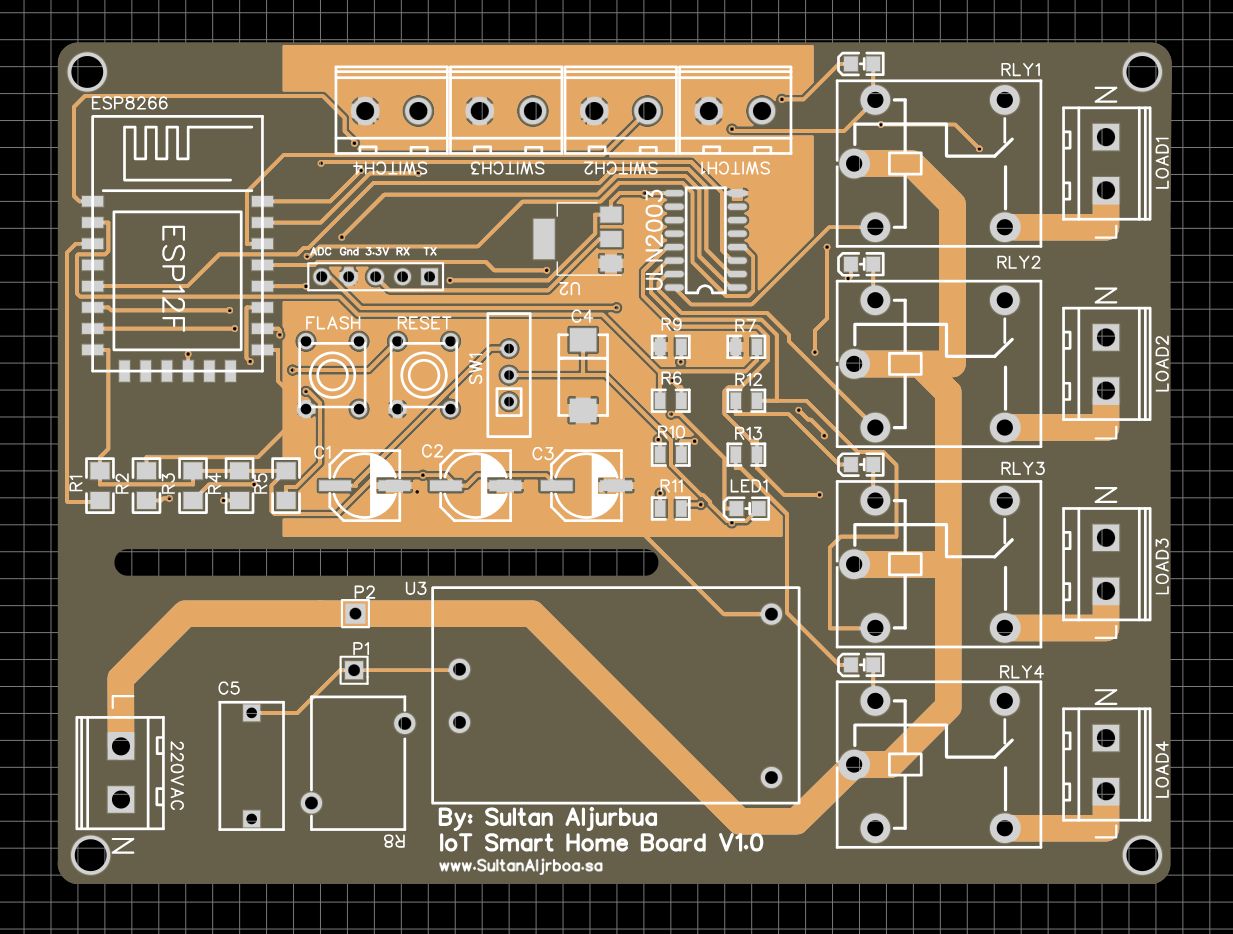
IoT Smart Home Automation prototype overview and system demonstration.
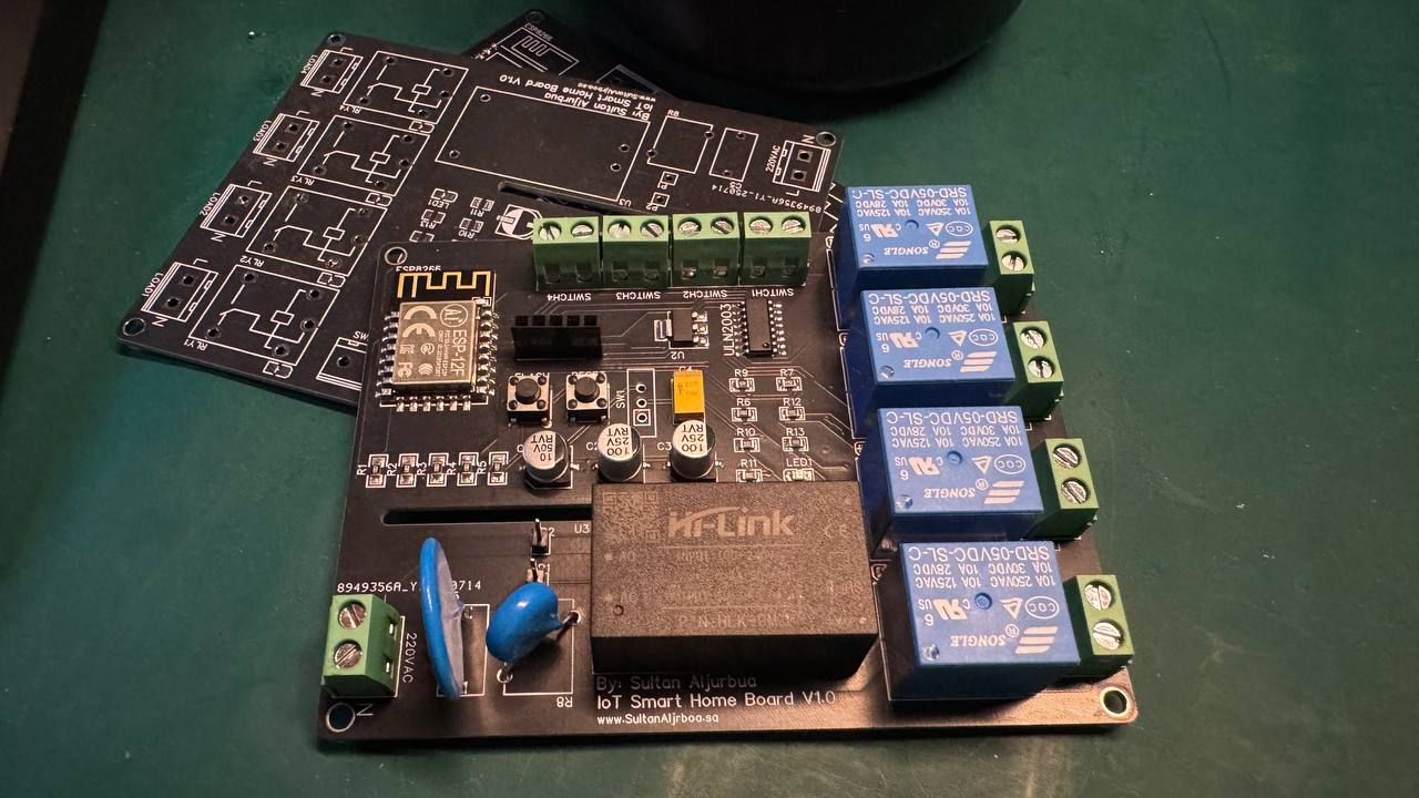
IoT Smart Home Automation is a PCB-based learning project focused on designing, manufacturing, soldering, and testing a real smart home control board. The board is built around the ESP8266 ESP-12F module and includes four relay channels for controlling electrical loads remotely.
Overview
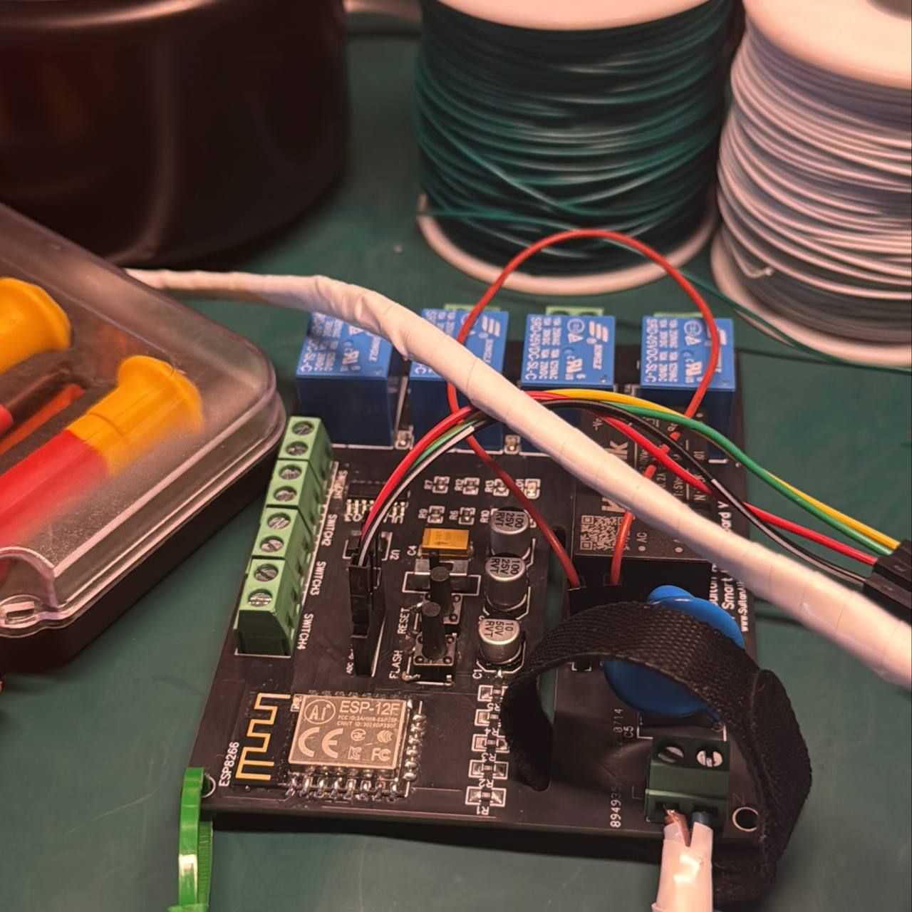
IoT Smart Home Automation is a custom PCB-based project designed to control home devices remotely. The main goal of the project was to gain hands-on experience in electronics design, PCB manufacturing, soldering, and real hardware testing.
- Custom smart home control board.
- Built around the ESP8266 ESP-12F Wi-Fi module.
- Includes four relay channels for device control.
- Designed as a practical learning project in PCB design and electronics assembly.
Project Goal
The main goal was not only to build a smart home board, but to understand the full hardware development workflow from schematic design to final operation. The project helped bridge the gap between theory and practical electronics implementation.
- Learn schematic design and PCB layout workflow.
- Understand how ESP8266-based IoT boards are designed.
- Practice through-hole and SMD soldering.
- Test a real working PCB instead of only simulating the circuit.
Design & Manufacturing Workflow
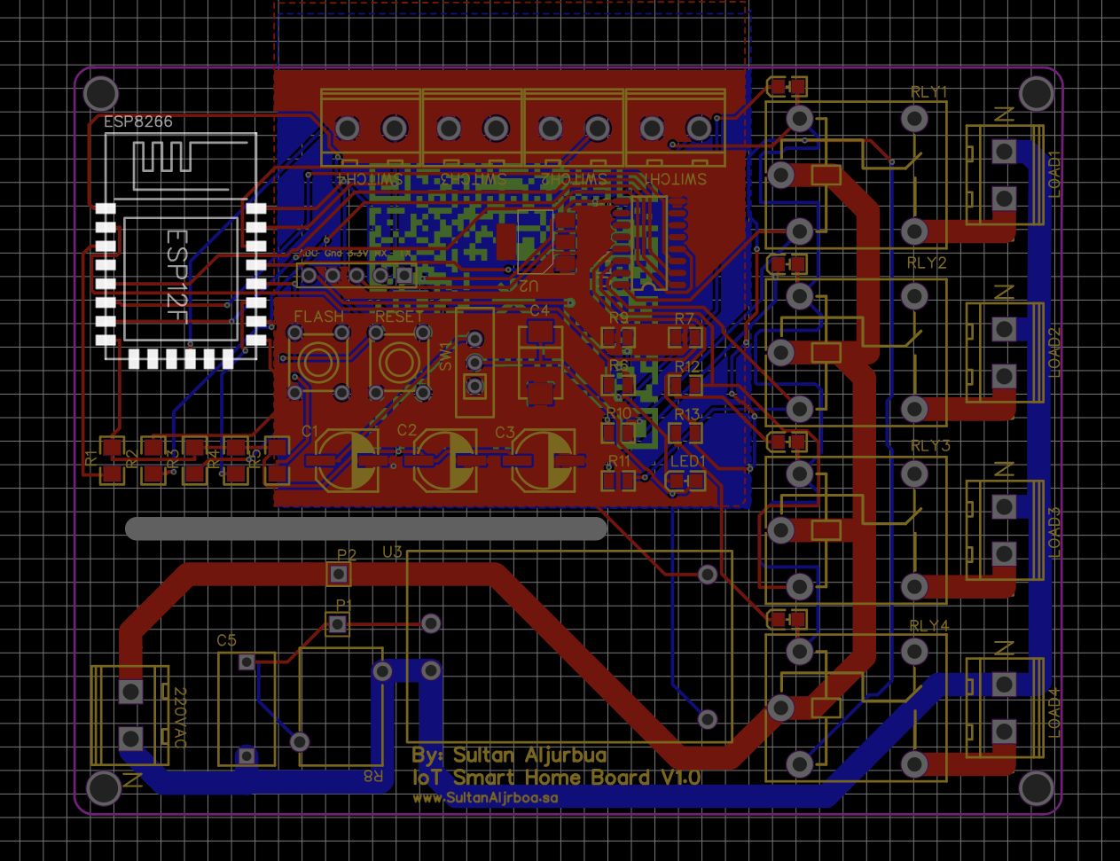
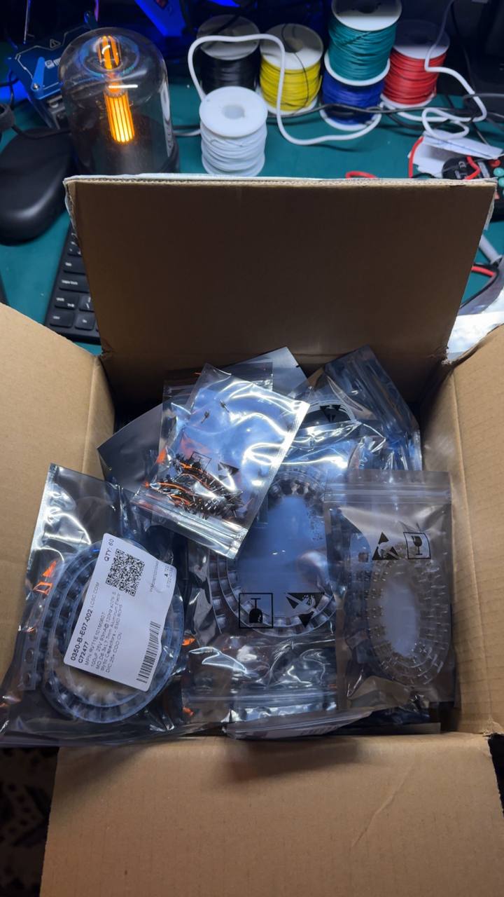
The project followed a complete hardware development process starting from schematic design using EasyEDA, then PCB layout, manufacturing, component preparation, soldering, and final testing. This workflow provided a practical understanding of how electronic products move from an idea to a physical board.
- Schematic design using EasyEDA.
- PCB layout and routing.
- Manufacturing the custom PCB.
- Component soldering and inspection.
- Final board operation and testing.
Hardware Architecture
The board is based on the ESP8266 ESP-12F module and includes four relays for switching external loads. The PCB also includes multiple connectors, power input, relay output terminals, control buttons, and supporting components required for operation and testing.
- ESP8266 ESP-12F Wi-Fi module.
- Four relay outputs for load control.
- AC input and load terminal blocks.
- Control switches and reset/flash buttons.
- Supporting capacitors, resistors, ICs, and protection components.
Lab Testing & Assembly
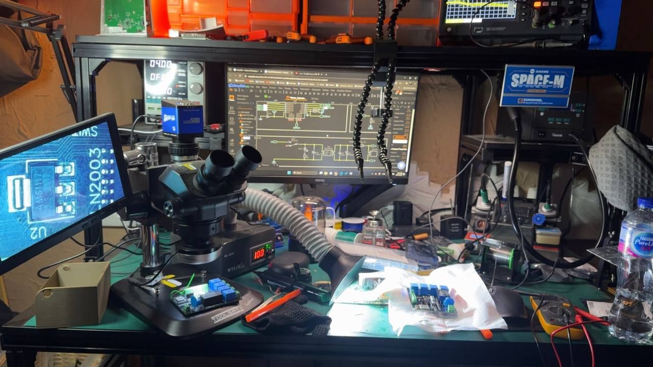
All assembly and testing were carried out in a personal electronics lab. The work included component preparation, soldering, SMD inspection under the microscope, continuity checks, and functional testing of the board.
- Practiced SMD soldering under the microscope.
- Verified solder joints and component placement.
- Tested power and relay behavior.
- Validated the board as a real working hardware prototype.
Key Learnings
This project was mainly a learning-focused hardware experience. It helped build confidence in PCB design, electronics assembly, practical debugging, and the process of converting a circuit design into a physical smart home control product.
- Understanding schematic design and PCB layout.
- Improving practical soldering skills.
- Learning how manufacturing files translate into a real PCB.
- Connecting IoT concepts with physical relay-based control.
- Planning future improvements for a more refined board version.